Photo-Induced Acoustoelectric Effect in High Resistivity Semiconductors - Methods of Deep Centers Investigation
P. Bury a, P. Hockicko a and I. Jamnický a
a Department of Physics, Žilina University, 010 26 Žilina, Slovakia
An interaction between an acoustic wave and free carriers in interface region of semiconductor structures has been proved to be an effective tool for the experimental investigation of deep centers. In high resistivity and along with photosensitive semiconductors the interface with space charge inhomogenity can be produced by the suitable non-uniform illumination of the sample with the weakly absorbed light. Applying a high frequency external electric field on interface region in proper conditions can then directly generate the longitudinal, transversal or surface acoustic wave. The time development of such generated acoustic wave amplitude is investigated to determine the deep centers parameters. The possibility to detect the deep centers by this way depends, however, on both the type and polarization of generated acoustic wave. In the contribution some experimental procedure is described and deep centers investigation for various generated acoustic waves in high resistivity GaAs sample are presented and compared.
introduction
An acoustoelectric effect on light been generated interface in high resistivity GaAs semiconductor has been shown [1] to be an effective method to study deep traps centers that can play an important role in a substrate materials used for opto- and micro-electronic devices. This new method in connection with acoustic transient spectroscopy (A-DLTS) can extend a number techniques used to study deep centers in high resistivity semiconductors [2-4].
In the present work we describe the technique of acoustic transient spectroscopy based on the utilization of space charge inhomogenity in high resistivity GaAs produced by non-uniform illumination. The space charge inhomogenity can generate in proper conditions both the longitudinal and transversal or surface acoustic wave by applying a high frequency electric field [5].
The basic idea of the used acoustic transient technique consists in the analysis of the amplitude time development of such generated acoustic wave after the light is turned off that is detected by the receiving transducer. The trap states inside the semiconductor band gap are either filed or emptied by an external stimulus, such as an optical illumination. After the external stimulus is removed, the traps either emit or capture charges to move forwards their equilibrium state.
The acoustic transient spectroscopy (A-DLTS) technique was applied to study deep centers for different acoustic waves with various polarization and/or propagation direction and obtained A-DLTS spectra are compared.
Experimental principle
Illuminating the part of high resistivity semiconductor by weakly absorbed light of proper energy, free carriers are produced. These photo-excited free carriers that alter the population of trapping centers by filling or emptying the trap levels for electron and/or holes, can immigrate from the illuminated to dark part of semiconductor producing the space charge region followed by internal arising of the internal electric field. When the illumination is turned off the photo-excited carriers recombine thereby establishing their thermal equilibrium.
The release of carriers from deep trap levels that leads to the thermal equilibrium on a new steady state has the dependence on time [6]
D n ( t ) = n t0 exp ( -t / t ) , (1)
where Dnt0 represents the variation in trap occupancy due to the acoustoelectric field and t is the time constant associated with the release of the carriers from deep centers when illumination is turned off. Since the amplitude of interface acoustic wave is proportional to the nonequilibrium carrier density at the semiconductor interface the decay time constant associated with the relaxation of the acoustic wave amplitude is a direct measure of t.
Using the well known relation expressing the temperature dependence of the relaxation time characterizing the acoustoelectric transient [6], the activation energies, trap density, and corresponding capture cross-sections can be determined.
Experimental results
The experimental arrangement and the principle of A-DLTS technique based on the computer evaluation of isothermal acoustoelectric transients used in this work for the determination of deep centers parameters have been already described [6, 7]. The light pulses of 200 ms width filling centers completely were applied to the investigated high resistivity Cr-doped GaAs sample through the metal screen using the IR-LED with the maximum in spectral characteristic of 900 nm.
The fast and slow mode of transverse acoustic wave (T1 and T2) and longitudinal acoustic wave (L) of frequency 13 MHz were generated through the acoustoelectric effect on space charge inhomogenity by applying hf electric field pulses in <110> direction and detected by transverse and longitudinal quartz transducers, respectively. The surface acoustic wave (SAW) of frequency 5 MHz was generated in <001> direction and detected by IDT.
Using a method of computer evaluation of isothermal acoustoelectric transients by applying a data compression algorithm [6] the activation energies and corresponding capture cross-sections were be determined from transient measurements of acoustic waves amplitudes.
Fig. 1 represents A-DLTS spectra obtained for various acoustic waves and calculated from the isothermal the acoustoelectric transients.
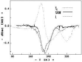
Figure 1 A-DLTS spectra of Cr-doped GaAs for transversal (T1), longitudinal (L) and surface acoustic wave (SAW)
The activation energies and corresponding capture cross-sections determined from the Arrhenius plots are summarized in Table 1.
Propagation |
Polarization |
Deep Centers |
|
|
Direction |
|
E [eV] |
s[cm2] |
|
[110]
[110]
[001] |
[001] (T1)
[110] (L)
(SAW) |
1.28 0.72 0.47 0.31 0.27 0.35 0.22 0.74 0.32 0.77 |
3.1x10⁻⁴ 2.4x10⁻¹³ 3.0x10⁻¹⁵ 4.8x10⁻¹⁸ 2.1x10⁻¹⁸ 1.7x10⁻¹⁶ 4.1x10⁻¹⁸ 5.1x10⁻¹² 2.0x10⁻⁷ 2.5x10⁻¹⁷ |
Table 1. Summary of the deep centers parameter detected in high resistivity GaAs for various acoustic waved
Most of the obtained energy levels of deep centers are in good agreement with the values found by the other techniques [8-10] that have been already compared and discussed [1].
Comparing the results obtained for different acoustic waves (T1, T2, L, SAW) generated on the same sample and mostly for the same screen indicates that the interaction of acoustic wave and deep centers depends both on the propagation direction and polarization of generated acoustic wave. Further study of this effect can give more complete information about the deep centers
In conclusion, we have demonstrated that the acoustic waves generated on light produced inhomogenity can be used in acoustic transient spectroscopy to study deep centers in high resistivity semiconductors and can give the useful information concerning the deep centers character.
Acknowledgements
The author would like to thank Dr. I. Turek for sample providing and Mr. F. Černobila for technical assistance. This work was partly supported by Grant No. 1/8308/01 of Slovak Ministry of Education.
References
1. P. Bury, Spectroscopy of Deep Centers in High Resistivity GaAs Using Light Beam Generated Interference in Proc. 16th Int. Congresson Acoustics, Seattle, 1998 Volume I, pp. 431-432
2. A. L. Lin and R.M. Bube, J. Appl. Phys. 47, 1859-1867 (1976)
3. P. M. Mooney , J. Appl. Phys. 54, 208-213 (1983)
4. Y. Mita, S. Sugata and N. Tsukada, Appl. Phys. Lett. 43, 841-843 (1983)
5. J. Braciník and J. Štelina, J. Appl. Acoustics 44, 369-374 (1995)
6. P. Bury and I. Jamnický, acta phys. slovaca 46 693-700 (1996)
7. P. Bury, I. Jamnický and V.W. Rampton, Physica B 263-264, 94-97 (1999)
8. G.M. Martin, A. Mitonneau and A. Mircea, Electronics Lett. 13, 191-192 (1977)
9. S. T. Pantalides, Deep Centers in Semiconductors, Gordon and Breach Science Publishers, ch.4, pp. 379-406 (1992)
10. F. Dubecký, J. Safránková and B. Olejníková, Crystal Properties &Preparation 12, 147-152 (1987)
11. A.L. Lin and R.H. Bube, J. Appl. Phys. 47, 1859-1867 (1976)